IC / ASIC Design Services

EnSilica provide an extensive set of full-flow IC design services focused on supporting semiconductor and systems companies in the delivery of IC, SoC, ASIC or FPGA projects.  These services range from a full turnkey solution that delivers a production ready design, to sub-system or IP block development, or having a our engineers augment your existing design teams with specialist design, application or EDA tools expertise.

Our services can be delivered using the wide range of 3rd party EDA tools we have in-house or by accessing our customer EDA licenses via VPN.  Our combination of European and Indian based design centres mean that we can form a team that offers the right balance of experience, scale and cost to meet the demands of any project.

Explore some of our recent projects in the Customer Case Studies section and also read what our customers say in our Customer Testimonials section.

Systems Level Design

Our specification development services start with our customer’s high-level marketing specification to finish with a complete system architecture and executable model, including a set of detailed technical specifications from the top-level to individual modules. Our experienced algorithms team are skilled in modelling RF and control systems and developing full system level models to prove the architecture before starting the detailed design.

Physical Implementation and DFT

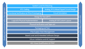
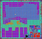
Our team of highly experienced implementation and Design-for-Test (DFT) engineers use a best in class design flow that uses either Synopsys IC Compiler II or Cadence Innovus Implementation System for physical design, the Mentor Tessent Suite for DFT, and Mentor Calibre for physical verification and sign-off. Our services range from RTL-to-GDSII block-level implementation for mixed signal analog-on-top design to hierarchical digital design in leading edge nodes.

We have experience with a variety of process nodes from 350nm to 12nm FinFet as well as the FD-SOI based process. Our foundry experience includes working with TSMC, Global Foundaries, UMC, SMIC and Key Foundry.

Our team has experience in low-power implementation using UPF (Unified Power Format), integration of RF IPs such as Wi-Fi and BLE (Bluetooth Low-Energy) as well as the integration and testing of high speed SerDes (Serializer/Deserializer) interfaces and data converters.

FPGA Design

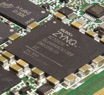
EnSilica has the in-house skills needed to develop, verify and take to market complex, reliable FPGA-based product for the most demanding markets. Experience includes development products for communication systems, automotive and industrial application using Xilinx, Intel (Altera) and Lattice FPGAs.

Our teams’ skills cover DSP and system design, RTL design, IP integration, high speed board design and embedded software. This includes SoC-based FPGAs incorporating multiple Arm cores and high-speed interfaces such as the latest Xilinx Virtex UltraScale+ devices. We apply the latest verification, linting and timing analysis methodologies to reduce the time spent hunting bugs on the bench and to improve reliability and quality.

We can help specify and develop FPGA firmware and embedded software to meet various functional safety standards, including industrial (IEC 61508) and automotive (ISO 26262) markets.

Read more

PCB Design

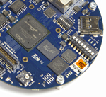
Our hardware team have experience in designing boards for both high volume production and for silicon evaluation. These boards include high-speed interfaces such as PCIe and DDR4, and RF connectivity including LoRa, BLE and NFC.

We have a vast amount of experience designing boards incorporating custom ASICs and Xilinx, Intel and Lattice FPGAs as well as designing with embedded processors from vendors including Nordic, ST, TI and NXP.  This includes developing a standard SoM product, eSi-ZM1, based on Xilinx Zynq device.  Recent projects have included: a LoRa (long Range) temperature sensor with NFC for configuration, a gas sensor for the oil and gas industry, and a high-resolution long-range Radar system and engine management monitoring unit with cellular communication for use in motor sports.

Read More

Design and Verification

Our services include the development of RTL for a wide range of applications including networking, wireless and Radar. Our team have the skills to develop new algorithms or implement designs from customer MATLAB or SystemC models.

EnSilica provide a comprehensive range of verification services to achieve right first time silicon. We apply a range of techniques including coverage driven constrained random verification using UVM with SystemVerilog. Our verification experience includes using  VIPs to verify complex interfaces such as PCIe and 10/100Gb Ethernet, UPF for multiple power down systems and the verification of complex AMBA bases bus systems with embedded processor cores.  We have experience in the verification of both multi-processor digital and mixed signal chips.

Analog Design and Layout

Our analog team are experienced in developing ultra-low-power SoCs and IP with integrated radios and power management that target nano-Amp sleep budgets in process nodes down to 7nm. RF based application areas include broadcast radio receivers, medical monitoring devices and wireless hearing aids incorporating custom and standards based sub-GHz and GHz radios. Standards based radio designs include BLE, BT Classic, Wi-Fi and 802.15.4/6.

Our experience in developing a wide-range of low-power ASICs has enabled us to build a broad library of silicon proven IPs including sensor interfaces, ADCs, DACs, SMPSs, LDOs, PLLs, temperature sensors and oscillators as well as BLE Radio and NFC AFEs.

Recent analog projects range from a Ka-band mmWave RF ASIC in 40nm CMOS for a satellite terminal to high performance radio chips in 350nm SiGe technology and an H-Bridge controller for an ASIL-D automotive application fabricated  in a 180nm BCD (Bipolar CMOS DMOS) process.

Embedded Software

Our software team support pre-silicon verification, post-silicon validation, and the development of production-quality software for a range of applications, including cellular and IoT (physical and protocol layers), networking, video, and radar signal-processing.

Recent processor platforms have included Arm Cortex® (A53, R5, M4/M3/M0), Tensilica’s ConnX BBE16, and NVIDIA GPU. Projects have been developed using embedded Linux or microkernels such as Arm Mbed, Micrium uCoS/III, and FreeRTOS as well as bare-metal developments.

Our safety-critical projects follow the V-model for rigorous design and testing and use the latest test methodologies to ensure thorough coverage.

Recent projects include an automotive radar system, low-power IoT modules using LoRaWAN, a safety-critical industrial controller, and USB sensors interface for mobile phones.

Silicon Validation

Our hardware, FPGA, software and lab engineers are skilled in efficiently validating that your ASIC meets the specification over process, temperature and voltage corners (PVT). This requires the development of automated test using LabVIEW, LabWindows or Python for controlling analogue and RF functions and an FPGA platform for controlling digital functions. We have developed an FPGA platform and methodology to accelerate this process and allow for testing as well as running your Scan and MBIST vectors on the ASIC ahead of bringing them on the production test platform. EnSilica has a well-equipped lab including oscilloscopes, spectrum analysers, logic analysers, signal generators and thermal chambers.

Find Out More

If you are looking for a trusted IC design partner with the right expertise and experience to bring your next product to market quickly and efficiently then please get in touch for an initial discussion.

© Copyright - EnSilica | Privacy Notice | Call Us - UK General : +44 118 321 7310 - UK Sales : +44 118 380 5757 - USA : +1 855 642 1070 - India : +91 80 2258 4450